Semeconductor 半导体
the-semiconductor-ecosystem
半导体行业组成:
- Chip Intellectual Property (IP) Cores
- Electronic Design Automation (EDA) Tools
- 该行业由三个美国供应商主导–Cadence、Mentor(现在是西门子的一部分)和Synopsys
- 一个使用这些EDA工具的大型工程团队需要2-3年的时间来设计一个复杂的逻辑芯片
- 随着芯片变得越来越复杂,开始插入人工智能辅助工具来自动化加快芯片设计流程。
- Specialized Materials
- Silicon wafers(硅晶晶圆) – and to make those they need crystal growing furnaces
- Over 100 Gases are used – bulk gases (oxygen, nitrogen, carbon dioxide, hydrogen, argon, helium), and other exotic/toxic gases (fluorine, nitrogen trifluoride, arsine, phosphine, boron trifluoride, diborane, silane, and the list goes on…)
- Fluids (photoresists光刻胶, top coats涂料, CMP slurries)
- Wafer handling equipment, dicing
- Wafer Fab Equipment (WFE)
- 五家公司主导行业:Applied Materials, KLA, LAM, Tokyo Electron and ASML
- 是地球上最复杂(也是最昂贵)的机器
- “Fabless” Chip Companies
- Integrated Device Manufacturers (IDMs)
- 新的前沿芯片 (3nm) 流片的平均成本现在为 5 亿美元
- Chip Foundries
- They design unique processes using this equipment to make the chips,But they don’t design chips
- TSMC 台积电 is the leader in logic, Samsung 三星 is second
- Fabs are short for fabrication plants – the factory that makes chips
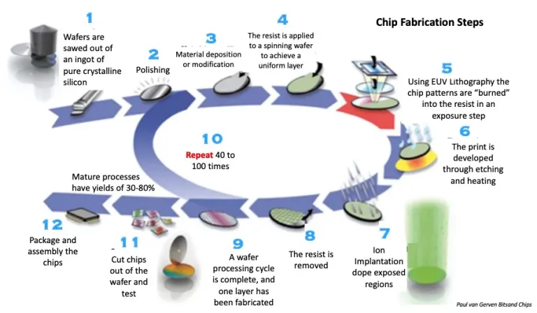
- Chips are probably the most complicated products ever manufactured. The diagram below is a simplified version of the 1000+ steps it takes to make a chip:
- Outsourced Semiconductor Assembly and Test (OSAT)


Fabs issue
- 建造晶圆厂的成本飙升——现在一个芯片工厂的成本超过 100 亿美元。原因之一是制造芯片所需的设备成本飙升
- 荷兰ASML公司的一台先进光刻机就耗资1.5亿美元
- There are ~500+ machines in a fab (not all as expensive as ASML)
- 晶圆厂建筑非常复杂。制造芯片的洁净室只是一组复杂管道的冰山一角,这些管道在正确的时间和温度下将气体、电力、液体全部输送到晶圆厂设备中
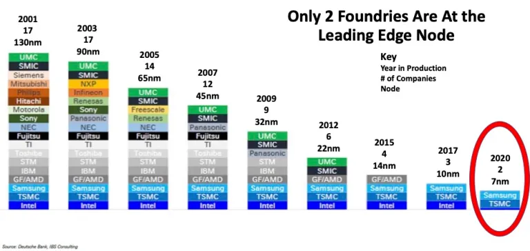
- 保持领先的成本高达数十亿美元,这意味着大多数公司已经退出了。2001年,有17家公司在生产最先进的芯片,今天只有两家:三星和台积电。